KAWARADA, Hiroshi
| Title | Professor |
|---|---|
| Affiliation | Department of Electronic and Physical Systems, Department of Nano-science and Nano-engineering |
| Research Area | Carbon Nanoelectronics, Power Elctronics, Biosensor, Superconducting Device |
| Research Interests |
Due to its extreme properties, diamond and carbon nanotube are expected to be applied in the ultimate semiconductor devices in high power, high temperature, high frequency operation and highly integration. In diamond, we focused on 2 dimensional hole gas (2DHG) layer appearing on a hydrogen terminated diamond surface and developed surface channel field effect transistors (FETs). This type of FET is applicable in high power and high-frequency devices, in-plane- gate FETs for single hole transistor, and biosensors in electrolyte solution. We are also investigating carbon nanotube for the multi layer interconnection for the next generation ULSI and ultimate electrode for SiC power transistors. In research, we worked on nanoelectronics from RF & power devices, superconductor devices, biosensors, bioelectronics and ULSI fabrication process based on nanocarbon electronics. The work covers the following area: 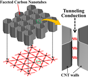 |
| Publications | https://waseda.pure.elsevier.com/en/persons/hiroshi-kawarada |
| Web | http://www.kawarada-lab.com/english/index.html |